- 您现在的位置:买卖IC网 > Sheet目录3753 > ATMEGA169P-16MUR (Atmel)IC MCU AVR 16K 16MHZ IND 64QFN
131
8018P–AVR–08/10
ATmega169P
When a capture is triggered according to the ICES1 setting, the counter value is copied into the
Input Capture Register (ICR1). The event will also set the Input Capture Flag (ICF1), and this
can be used to cause an Input Capture Interrupt, if this interrupt is enabled.
When the ICR1 is used as TOP value (see description of the WGM13:0 bits located in the
TCCR1A and the TCCR1B Register), the ICP1 is disconnected and consequently the Input Cap-
ture function is disabled.
Bit 5 – Reserved Bit
This bit is reserved for future use. For ensuring compatibility with future devices, this bit must be
written to zero when TCCR1B is written.
Bit 4:3 – WGM13:2: Waveform Generation Mode
See TCCR1A Register description.
Bit 2:0 – CS12:0: Clock Select
The three Clock Select bits select the clock source to be used by the Timer/Counter, see Figure
If external pin modes are used for the Timer/Counter1, transitions on the T1 pin will clock the
counter even if the pin is configured as an output. This feature allows software control of the
counting.
15.11.3
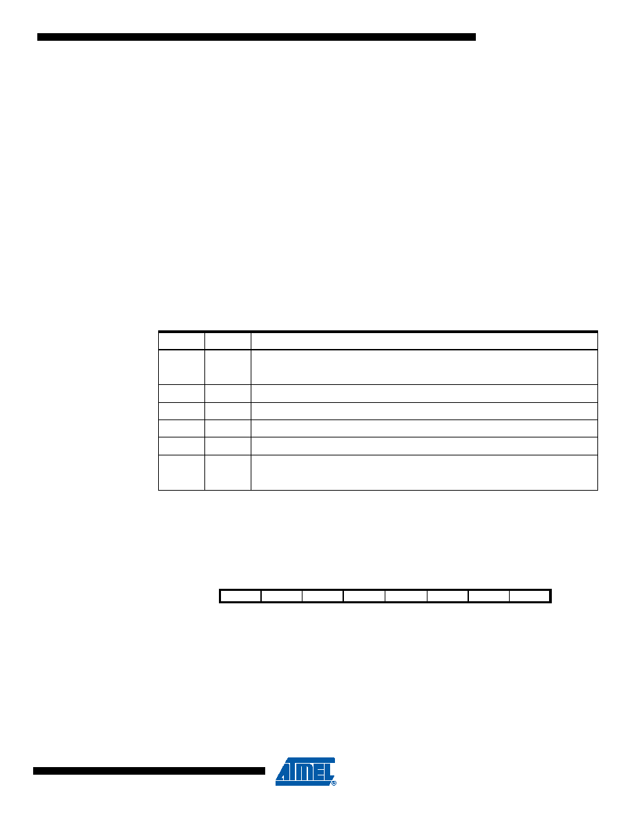
TCCR1C – Timer/Counter1 Control Register C
Bit 7 – FOC1A: Force Output Compare for Unit A
Bit 6 – FOC1B: Force Output Compare for Unit B
The FOC1A/FOC1B bits are only active when the WGM13:0 bits specifies a non-PWM mode.
However, for ensuring compatibility with future devices, these bits must be set to zero when
TCCR1A is written when operating in a PWM mode. When writing a logical one to the
FOC1A/FOC1B bit, an immediate compare match is forced on the Waveform Generation unit.
The OC1A/OC1B output is changed according to its COM1x1:0 bits setting. Note that the
Table 15-5.
Clock Select Bit Description
CS12
CS11
CS10
Description
0
No clock source (Timer/Counter stopped).
00
1
clkI/O/1 (No prescaling)
01
0
clk
I/O/8 (From prescaler)
01
1
clkI/O/64 (From prescaler)
10
0
clk
I/O/256 (From prescaler)
10
1
clk
I/O/1024 (From prescaler)
1
0
External clock source on T1 pin. Clock on falling edge.
1
External clock source on T1 pin. Clock on rising edge.
Bit
765
4
3
210
(0x82)
FOC1A
FOC1B
–
TCCR1C
Read/Write
R/W
R
Initial Value
0
发布紧急采购,3分钟左右您将得到回复。
相关PDF资料
ATMEGA169P-16MCHR
MCU AVR 16KB FLASH 16MHZ 64-VQFN
2-1546217-0
TERM BLK RCPT 20POS SIDE 5.08MM
1-1546217-9
TERM BLK RCPT 19POS SIDE 5.08MM
1-1546217-8
TERM BLK RCPT 18POS SIDE 5.08MM
1-1546217-7
TERM BLK RCPT 17POS SIDE 5.08MM
1-1546217-6
TERM BLK RCPT 16POS SIDE 5.08MM
1-1546217-5
TERM BLK RCPT 15POS SIDE 5.08MM
1-1546217-4
TERM BLK RCPT 14POS SIDE 5.08MM
相关代理商/技术参数
ATMEGA169P-8AU
制造商:ATMEL 制造商全称:ATMEL Corporation 功能描述:Microcontroller with 16K Bytes In-System Programmable Flash
ATMEGA169P-8MU
制造商:ATMEL 制造商全称:ATMEL Corporation 功能描述:Microcontroller with 16K Bytes In-System Programmable Flash
ATMEGA169PA
制造商:ATMEL 制造商全称:ATMEL Corporation 功能描述:8-bit Microcontroller with 16K Bytes In-System Programmable Flash
ATMEGA169PA_1
制造商:ATMEL 制造商全称:ATMEL Corporation 功能描述:High Endurance Non-volatile Memory segments
ATMEGA169PA-AN
功能描述:8位微控制器 -MCU AVR XMEGA 384KB 105C 4KB EE32K SRAM-16MHz RoHS:否 制造商:Silicon Labs 核心:8051 处理器系列:C8051F39x 数据总线宽度:8 bit 最大时钟频率:50 MHz 程序存储器大小:16 KB 数据 RAM 大小:1 KB 片上 ADC:Yes 工作电源电压:1.8 V to 3.6 V 工作温度范围:- 40 C to + 105 C 封装 / 箱体:QFN-20 安装风格:SMD/SMT
ATMEGA169PA-ANR
功能描述:8位微控制器 -MCU AVR XMEGA 384KB 105C 4KB EE32K SRAM-16MHz RoHS:否 制造商:Silicon Labs 核心:8051 处理器系列:C8051F39x 数据总线宽度:8 bit 最大时钟频率:50 MHz 程序存储器大小:16 KB 数据 RAM 大小:1 KB 片上 ADC:Yes 工作电源电压:1.8 V to 3.6 V 工作温度范围:- 40 C to + 105 C 封装 / 箱体:QFN-20 安装风格:SMD/SMT
ATMEGA169PA-AU
功能描述:8位微控制器 -MCU AVR XMEGA 384KB FLSH 4KB EE32K SRAM-16MHz RoHS:否 制造商:Silicon Labs 核心:8051 处理器系列:C8051F39x 数据总线宽度:8 bit 最大时钟频率:50 MHz 程序存储器大小:16 KB 数据 RAM 大小:1 KB 片上 ADC:Yes 工作电源电压:1.8 V to 3.6 V 工作温度范围:- 40 C to + 105 C 封装 / 箱体:QFN-20 安装风格:SMD/SMT
ATMEGA169PA-AUR
功能描述:8位微控制器 -MCU AVR LCD 16KB FLSH EE 512B 1KB SRAM-16MHZ RoHS:否 制造商:Silicon Labs 核心:8051 处理器系列:C8051F39x 数据总线宽度:8 bit 最大时钟频率:50 MHz 程序存储器大小:16 KB 数据 RAM 大小:1 KB 片上 ADC:Yes 工作电源电压:1.8 V to 3.6 V 工作温度范围:- 40 C to + 105 C 封装 / 箱体:QFN-20 安装风格:SMD/SMT